Motor controller
Every electric bike needs a motor controller to very precisely turn the motor.
The controller accepts many inputs (such as throttle voltage, break indicator, ...) and turns the motor accordingly.
CUX, TC, TSX
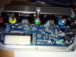
These bikes are confirmed to use the Lingbo-mc LBMCHK2AE motor controller ver. 1.0
This controller has 3 motor phases U, V and W. 2 more terminals deliver battery voltage. Underneath there is a 30pin connector used to communicate with the rest of the bike and get inputs from the many sensors.
The unit is powered by the STM32 F030C8 microcontroller. The manufacturer attempts to prevent tampering by using RDP (read-out protection) level 1. This protection level still allows to attach a debugging interface, but disconnects the flash memory every time you do so.
Additionally, the controller uses 3PEAK TP8485E to communicate via RS-485 bus. This chip simply provides translation between the internal UART of the STM32 and the external RS485 that the bike uses for everything.
Not fitted with a proper header, there is also a 4pin JTAG interface consisting of 3.3V+, CLK, GND and DIO. This header can be used to programm the STM32 and to attach debugger.
Firmware upgrade
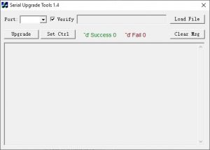
Legitimate firmware upgrade is performed with a "Serial Upgrade Tools" software. It is intended to be used with an official RS-485#Service cable.
Standard firmware upgrade procedure
- Shut down power breaker and disconnect 30pin connector from the controller
- Connect 30pin service connector to controller, connect data usb (silver) to computer
- Open software, load firmware, click Upgrade
- Connect power usb (black) to computer
- Firmware upgrade is performed
Upgrade sequence
You can observe the complete upgrade session as recorded by a COM port sniffer.
- When connected to the USB power cable, the controller first announces its presence.
- The computer respondes with a confirmation.
- The controller then announces it is ready for upgrade.
- The computer sends individual 1024B blocks of the firmware in the upgrade phase.
- After each block, the controller responds with a confirmation that the uploaded block was written. The command byte here is the same as the uploaded block's command, and 0x70 is used as successful status, 0x71 as unsuccessful.
- When reaching the end, the computer sends all the blocks again, this time as verification phase.
- After each block, the controller responds with a confirmation that the uploaded block matches the block that is present on the flash memory, using the same status confirmation as the upgrade phase.
Upgrade protocol
Generally, the upgrade procedure communicates using RS-485 messages with the following properties.
- 1st byte is always 0xE2
- 2nd byte is a command byte
- last byte is always a verification byte calculated by XORing all of the previous bytes in the message
We can deduce some of the commands:
| Command | Purpose |
|---|---|
| 0x00 - 0x3A | Upload block |
| 0xC5 - 0xFF | Verify block |
| 0x80 | Initial handshake |
| 0x81 | Firmware upgrade ready |
Analysis
Please note: From now on, we use the word block for both 1KB firmware blocks and 32B cipher blocks. Please mind the context.
The firmware itself is a 64KB (matching the size of the flash memory) file with variable amount of data that is padded with 0xFF towards the end. Different firmwares may contain different amount of data.
Interestingly enough, the firmware is not uploaded from the beginning, rather, the upload starts at address 0x1000 which is identified as block 0x00 (or 0xC5 in verification phase). We strongly believe that 0x0000 - 0x1000 contains the bootloader that might be upgraded in a different way, if ever.
Regardless of padding, there is a 64byte block at 0xEFC0 that contains an identification header.
The firmware file is encrypted with a yet unknown block cipher with following properties:
- block size 256bits
- full block scramble (altering one byte inside the block completely changes the whole block)
- no block chaining (altering one block doesn't affect any other blocks)
- block full of 0x00s or 0xFFs is left as plaintext
The attack preparations
To obtain the unencrypted firmware, several modifications had to be done to the device.
First of all, JTAG pins had to be soldered to the board, mostly just the CLK and DIO as the 3.3V and GND are already present on the 30pin connector.
Interestingly enough, the official service cable puts 5V from USB to the 3.3V pin of the STM32 chip, effectively running it out of specs.
However, when only 3.3V is applied to the chip, the RS485 announcement does not happen. It is therefore impossible to flash firmware using the intended way with the 3.3V power that the chip is supposed to have.
The assumed reason for this is that the RS485 chip is configured to operate on 5V and gives too weak of a signal when powered from 3.3V.
To overcome this, we had to solder another two header pins on the UART RX and TX pins between the STM32 and TP8485E. The TP8485E legs are an ideal spot for this. This way, we connected our UART adapter directly to the UART bus of the chip, effectively bypassing the RS485 bus altogether. This time, we were able to observe the upgrade handshake even when using 3.3V power, enabling us to use ST-LINK adapter to debug the chip. The UART and RS485 speed when upgrading is 115 200 baud.
The attack
Having this setup, we were able to write our own script that mimicked the firmware upgrade utility, but already on the UART bus.
When debugged, the chip halts and disconnects the flash memory, but the RAM remains intact. We discovered, that after every 1024B block that is sent (doesn't matter if upgrade or verify phase), the block is stored in the RAM at 0x620 as a receive buffer. Once fully received, the block is decrypted in-place.
The attack scenario is following
- Send a complete block of the firmware with a verify command (for example 0xC5)
- The controller will receive the block and decrypt it in RAM
- Attach the debugger
- Dump the contents of the RAM at 0x620
- Repeat for all blocks
This attack is pretty tedious because it requires constant reconnecting of the power to the chip to reset it into working condition before moving further with the next block. Nevertheless, there are only 64 blocks maximum and we are skipping the first 4 blocks for the bootloader, so this is doable in mere 15 minutes of manual work.
Another problem is that after every block, the controller sends the confirmation message. Unfortunatelly, the output buffer for that message is constructed at the same memory address 0x620, effectively overwriting the first 4 bytes of the now-decrypted block. This happens too fast to be able to prevent and attach the debugger before the confirmation is sent. This effectively leads to every decrypted block having the first few bytes unobtainable.
Luckily, the cipher doesn't chain its blocks, so in phase 2 of the attack, we construct arbitrary firmware block consisting of the first 32B of every block that was previously dumped, have it be decrypted by the firmware, and then fill in those missing bytes.
This way we are able to arbitrarily decrypt any given firmware file, or any given 32B block of data.

